
Overview
I am an experimental physicist and materials scientist specialising in advanced electron microscopy and the structure–property relationships of nanomaterials for energy and optoelectronic applications. My work combines high-resolution TEM/STEM and spectroscopy with optical and electrical measurements to understand how atomic-scale structure, defects and interfaces control device-relevant performance.
I have led research on confined halide perovskites (“picoperovskites”) in carbon nanotubes, 1D and 2D van der Waals heterostructures, and phase-change and thermoelectric materials. A recurring theme in my work is the use of encapsulation and confinement to stabilise otherwise fragile material phases and to engineer their optical and electronic response under realistic operating conditions.
Research Focus
- Atomic-scale electron microscopy (TEM/STEM, EELS) of functional materials
- Confined halide perovskites and “picoperovskite” nanostructures
- 1D radial and 2D van der Waals heterostructures
- Energy materials and optoelectronic devices (PV, photodetectors, memory)
- Correlative structure–optics–transport measurements in working devices
Selected Publications
Picoperovskites: the Smallest Conceivable Isolated Halide Perovskite Structures Formed Within Carbon Nanotubes
Advanced Materials, 2023.
R. J. Kashtiban, C. E. Patrick, Q. Ramasse, R. I. Walton, J. Sloan.
Linear and Helical Cesium Iodide Atomic Chains in Ultranarrow Single-Walled Carbon Nanotubes: Impact on Optical Properties
ACS Nano 15, 13389–13398 (2021).
R. J. Kashtiban et al.
Ultrafast Optoelectronic Processes in 1D Radial van der Waals Heterostructures
Nano Letters 20, 3560–3567 (2020).
M. G. Burdanova, R. J. Kashtiban et al.
Towards a 3D GeSbTe Phase Change Memory with Integrated Selector by Non-Aqueous Electrodeposition
Faraday Discussions 213, 339–355 (2019).
R. Huang, G. P. Kissling, R. Kashtiban et al.
Atomically Resolved Imaging of Highly Ordered Alternating Fluorinated Graphene
Nature Communications 5, 4902 (2014).
R. J. Kashtiban et al.
Research Highlights
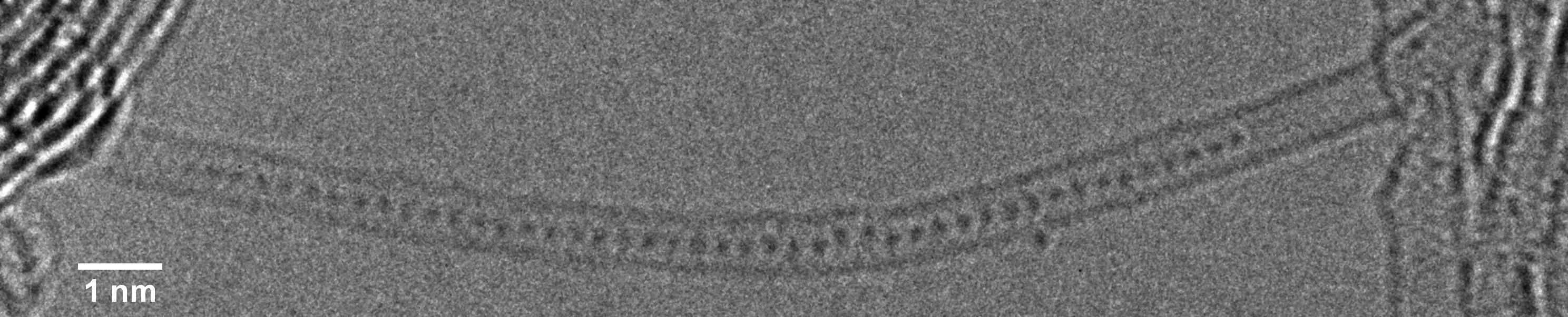 Confined Extreme Nanowires
Encapsulation of technologically important materials in ultranarrow templates to form 1D atomic chains and motifs with tunable properties and enhanced stability.
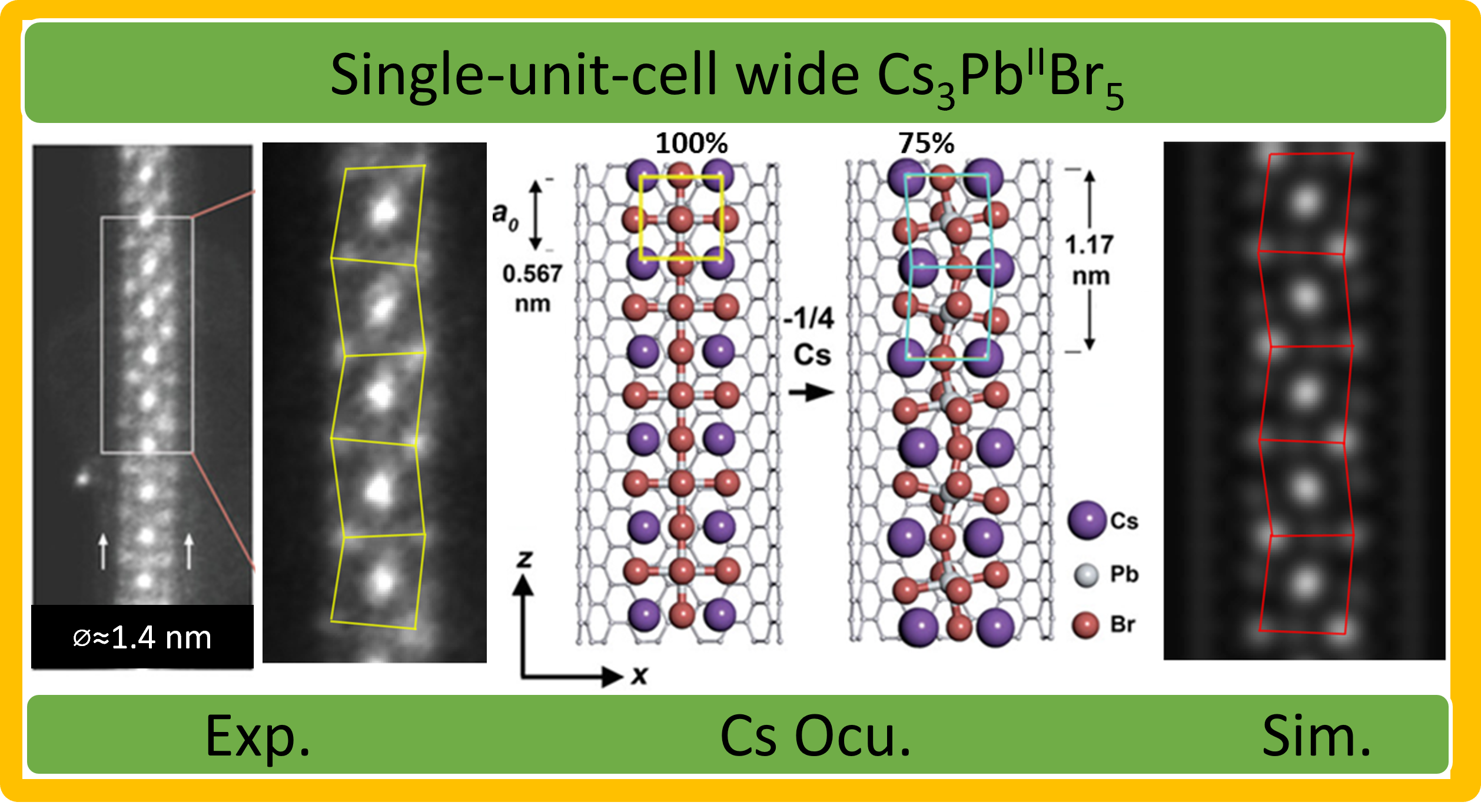
Confined halide perovskites and composite 1D heterostructures enabling tunable optoelectronic behaviour at the nanoscale.
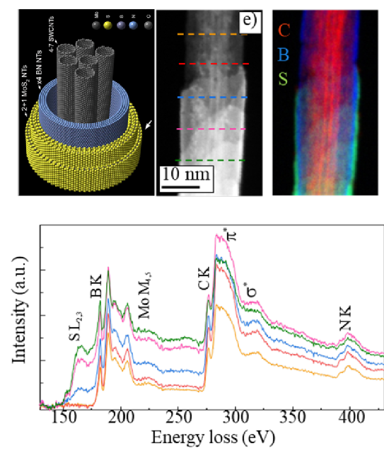 1D radial Van der Waals heterostructures
CNT/BN/MoS2 radial heterostructures supporting coexisting excitons and highly mobile charge carriers, enabling ultrafast optoelectronics at atomic scale.
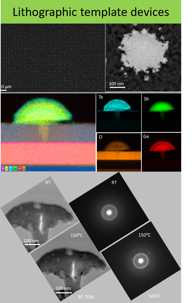 In situ microscopy of phase-change devices
Elemental mapping of nonvolatile GeSbTe memory cells and selectors, linked to device-scale electrical behaviour for improved reliability and scaling.
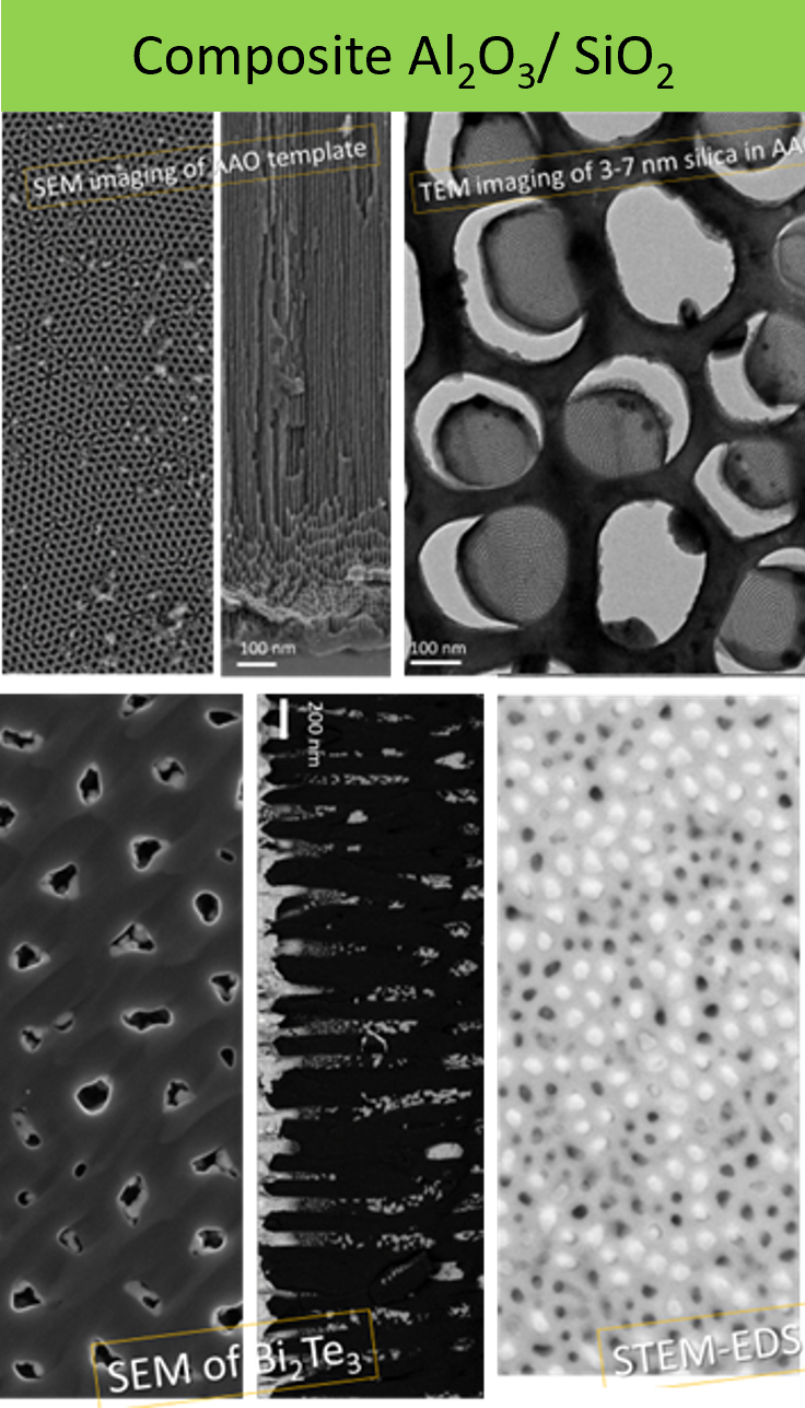 Templated thermoelectric nanowires
Template-directed synthesis and atomic-resolution characterisation of Bi2Te3 nanowires for thermoelectric and topological applications.
Teaching & Supervision
- Course design and delivery (UG/PG): Advanced Characterisation of Nanomaterials; Crystallography and Diffraction; Electron Microscopy and Spectroscopy; Optical Properties of Solids; Electricity and Magnetism; Superconductivity; Electrodynamics; Physics Laboratories; and UG/PG project modules.
- Teaching institutions: University of Warwick; University of Manchester; Urmia University (Iran).
- Supervision of BSc and MPhys final-year projects in electron microscopy and nanomaterials.
- Postgraduate training in TEM/STEM imaging, diffraction and spectroscopy.
- Research-informed teaching on the measurement and properties of matter, nanomaterials and devices.
Contact
Professional Contact
Dr Reza Kashtiban
Email: r.kashtiban@warwick.ac.uk
LinkedIn:
View profile
ORCID:
View ORCID record
Google Scholar:
View publications